|
The core of the experiment is the ANALOG DEVICES
ADIS16355 Inertial Measurement Unit. This is an highly integrated sensor
that has three accelerometers and three gyros, aligned over three
orthogonal axis, with the relative signal amplification and conditioning
embedded inside, and provides digital outputs over the SPI (Serial
Peripheral Interface) 3-wire bus. Moreover, the device comes already
factory calibrated and compensated over a wide temperature range
(-40÷+80°C).
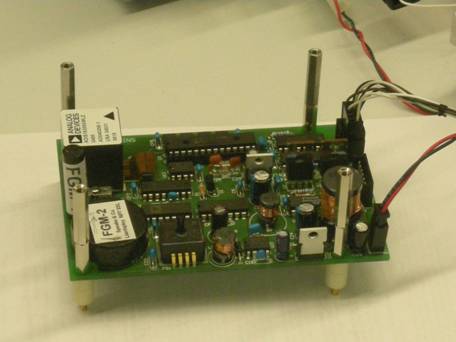
The magnetic field sensors (single-axis FGM-1,
two-axis FGM-2), built by “Speake & Co Llanfapley”, provides digital
output, as the output signal is a square wave whose period is directly
proportional to the field strength being measured. We chose to use
digital output sensors because they can be easily interfaced with the
microcontroller without need for any other components, moreover they
offer high noise immunity level.
The only analogue sensor is the Honeywell ASDX015A24R absolute pressure
sensor that is connected to an analogue port of the microcontroller.
However it provides a robust 4 V voltage span over the entire
measurement range.
Every sensor is connected to a Microchip PIC 18F2620 microprocessor. It
has 10 channel 10 bit ADC, hardware I2C, SPI, UART interfaces, as well
as counter modules. Data gathered from sensors are sent through RS232
interface to E-link TM/TC module. However the same RS232 interface can
be used for service purpose during on ground tests.
All data are also stored onboard on four ATMEL AT45DB161D 16Mbit flash
memories. Since they have 3-wire SPI interface compatible with ADIS16355
IMU, they can be easily connected together over the same SPI bus,
providing a simple circuit layout design.
The power supply, provided by battery pack, is regulated to 5 V and 3.3
V using a DC-DC converter..
In the following figure is represented an overall functional block
diagram of the experiment.


Below few pictures of LowCoINS
board.

|