Nelle macchine fotografiche
digitali la pellicola è sostituita da un sensore. Questo sensore non è altro
che un chip su cui l’immagine è catturata in analogico e convertita in
digitale.
Il sensore è diviso in milioni di
piccole aree chiamate pixel, ognuna delle quali registra l’informazione di
colore relativa a un’area molto piccola. Oggi i sensori raggiungono
facilmente risoluzioni enormi come tre milioni di pixel (il massimo è 14
milioni). In fotografia il numero di pixel si misura in Megapixel/Mp
(milioni di pixel). Il numero totale di pixel è calcolabile anche come
prodotto della massima risoluzione verticale per la massima risoluzione
orizzontale. Ad es. se la macchina riprende 1280x1024 = 1,3 Mp. Per eseguire
l’operazione contraria (massima risoluzione a partire dai Megapixel)
dobbiamo ricordarci che il rapporto standard tra la risoluzione orizzontale
e quella verticale è di 1,25:1. Quindi per prima cosa dobbiamo dividere il
numero di Mp per 1,25 poi calcolare la radice quadrata (otterremo la misura
minore: 1024) infine calcolare l’altra misura moltiplicando nuovamente per
1,25.
Quanto conta il numero di Mp
È importante notare che la
“definizione” aggiuntiva catturata da un CCD con più Mp potrebbe deludere
chi si aspetta un nettissimo cambiamento. Mi spiego meglio: passando da 2 MP
a 5Mp potreste pensare che un oggetto fotografato raddoppi (e oltre) la sua
dimensione e sia quindi stampabile a grandezza più che doppia. Es. potreste
pensare che un’immagine a 2Mp sia stampabile agevolmente a 9x12 e quella da
5Mp a 18x24. (Le cifre non sono accurate, sono scelte solo per dare un’idea
tangibile). Invece no. Infatti linearmente la risoluzione del CCD è
aumentata solo della radice quadrata di 5/2 e cioè di 1,6 volte! Ben meno
che 2,5 che ci saremmo aspettati a occhio.
Dunque se per definizione
intendiamo l’aumento di dettagli in entrambe le direzioni, i Mp sono
effettivamente un parametro utile che misura l’aumento di nitidezza
nell’immagine. Ma se ci interessa notare un particolare o stampare la foto
più che i Megapixel ci interessa la risoluzione orizzontale (o verticale) e
passando da un ccd all’altro quello che conta è la radice quadrata del
rapporto tra le dimensioni dei sensori in Mp.
Rapporti teorici e
Rapporti reali
Sensori
1 Mp
2 Mp
3 Mp
5 Mp
10 Mp
14 Mp
1 Mp
1
1
2
1,4
3
1,7
5
2,2
10
3,1
14
3,7
2 Mp
1
1
1,5
1,2
2,5
1,6
5
2,2
7
2,6
3 Mp
1
1
1,7
1,3
3,3
1,8
4,7
2,2
5 Mp
1
1
2
1,4
2,8
1,7
10 Mp
1
1
1,4
1,2
14 Mp
1
1
Come vedete i rapporti reali (tra
risoluzioni orizzontali) sono molto deludenti rispetto all’aumento di
Megapixel e sono tanto più deludenti (in percentuale) quanto più l’aumento è
forte. In altre parole se l’aumento dovrebbe essere del doppio in realtà è
di 1,4 volte. Ma se “dovrebbe” essere di 14 volte è di appena 3,7!
Grandezza dei sensori CCD
Un'altra caratteristica molto
importante per i sensori CCD è la grandezza: la grandezza dei singoli pixel
(più che del ccd) influisce moltissimo sulla capacità di catturare luce.
Sensori grandi (e quindi pixel più grandi) di norma hanno una resa dinamica
maggiore dei sensori piccoli. I valori più diffusi in ordine crescente di
grandezza sono 1/2.7", 1/1.8", 2/3", 23x15mm circa, 35x23mm (FF). La
grandezza effettiva del ccd si calcola esattamente come è facile ipotizzare.
Es 1/1.8" = 0.55" quindi 1/1.8 è più piccolo di 1/1.3.
Grandezze di ccd da 23x15mm circa a 35x23mm o superiori sono le più usate
dai professionisti.
Funzionamento
Il funzionamento fisico di un ccd
è qualcosa di complesso e poco interessante per un fotografo, vi basta
sapere che grazie all’elettronica è stato possibile costruire strutture
microscopiche in grado di rilevare l’intensità di luce che le colpisce
attraverso variazioni della corrente elettrica prodotta (o lasciata
passare). Il passo successivo è quello di convertire l’intensità di corrente
elettrica in un segnale digitale attraverso un convertitore AD
(Analogico-Digitale) a grande risoluzione di colore (12 bit, 16 bit).
Pixel Monocromatici
La cosa che è importante notare
però, è che ogni pixel cattura un solo colore. Esatto i pixel sono
monocromatici. In pratica i CCD attuali vengono “verniciati” pixel per pixel
con una vernice trasparente che permette a ogni pixel di catturare la luce
solo nella componente di colore di cui è verniciato. Per capire meglio
questa tecnica basta pensare all’effetto che si ha guardano attraverso un
filtro colorato. In pratica vediamo solo quel colore nelle sue diverse
intensità.
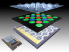
Lo schema
più usato consiste nel dipingere i pixel adiacenti secondo lo schema GRGB
Green (verde), Red (rosso), Blue (blu), Green (verde) (si noti che il verde
è il colore a cui l’occhio umano percepisce la maggior parte di dettagli). I
colori appena citati sono i colori primari, da questi è possibile ottenere
qualsiasi altro colore.
In pratica l’effetto che si
ottiene attraverso questa tecnica è quello di avere tre fotografie dello
stesso oggetto, ognuna leggermente spostata rispetto all’altra di una certa
misura angolare (che corrisponde a pochi millimetri o meno a distanze di
pochi metri). Il calcolo si effettua così: larghezza area fotografata alla
distanza X (ad es. circa 5 metri di larghezza a 5 di distanza)/risoluzione
orizzontale. Per un sensore a 3Mp abbiamo = 5 m / 1550 = 3mm.
Queste immagini vengono fuse
insieme attraverso un procedimento molto complesso che richiede, per dare
un’idea, circa 100 operazione per singolo pixel. Nonostante ciò il
procedimento produce artefatti abbastanza vistosi come una risoluzione
“reale” inferiore a quella dichiarata e raggiunta solo grazie
all’interpolazione, un certo livello di sfocatura necessario per evitare
artefatti di colore che si verificano comunque su superfici a mosaico (es.
una camicia).
Il sensore X3 della Foveon è
l’unico a non utilizzare questa tecnica e a catturare le immagini senza
artefatti di sorta.
Range Dinamico
Il Range Dinamico è il rapporto
tra la più forte e la più debole luce catturabile dal sensore ccd una volta
fissati tempo di otturazione, apertura diaframma e sensibilità iso. Il range
dinamico è quindi un sinonimo di contrasto massimo tra luce e ombra che
viene reso correttamente dal ccd. Anche l’occhio umano e la pellicola hanno
un range dinamico limitato, il fatto è evidente se si pensa all’effetto che
si ha guardando una pila che ci viene puntata in faccia o fotografando con
qualunque macchina in controluce. In pratica un range dinamico troppo
limitato ci porterà ad avere immagini con parti troppo chiare (sovraesposte),
troppo scure (sottoesposte) o addirittura entrambe. In queste aree perdiamo
completamente (o quasi) i dettagli e anche i migliori software faticano a
recuperarli (e se ci riescono spesso l’immagine non è certo gradevole).
Sotto, esempio di range dinamico
troppo basso.
Il range dinamico non viene
dichiarato dai costruttori, ma può essere misurato attraverso alcuni test,
la misura è espressa in ev (equivalent value) o in rapporti di contrasto
(es. 400:1). Questo range varia inoltra al variare della sensibilità iso
impostata, avendo il valore massimo per iso bassi (100) e calando
rapidamente per valori alti (a iso 800 è in media 4 volte più basso che a
iso 100). Nella maggior parte degli apparecchi il range dinamico a iso 100
spazia tra 100 e 400, a secondo del modello.
Il nuovo sensore inventato da
Fujifilm (il superCCD S3) è il migliore in questo campo sebbene guadagni
solo il 25/30% in più rispetto ai migliori ccd tradizionali. La tecnologia è
comunque ancora giovane e il range dinamico è una delle caratteristiche più
importanti per un fotografo (anche e soprattutto per quelli alle prime erbe)
Convertitore AD
Come ho detto i pixel sono
misuratori analogici e la misura da loro prodotta è un segnale elettrico
misurabile in volt. Tale segnale deve essere convertito in digitale. La
conversione introduce un fenomeno di perdita d’informazione chiamato “quantizzazione”.
Questo fenomeno è dovuto al fatto che il numero di bit usati per ogni pixel
è molto piccolo e il numero di informazioni codificabili con N pixel è 2N.
Nella maggior parte delle fotocamere abbiamo N = 8 e di conseguenza 2N=
256. Ciò significa che qualsiasi immagine fotografiamo dovremo descriverla
con “solo” 256 gradazioni di luminosità (per ogni colore). Le ultime
fotocamere professionali hanno 10 o addirittura 12 bit che corrispondono
rispettivamente a 1024 e 4096 gradazioni.
È utile? Beh diciamo di sì ma
molto, molto meno delle altre caratteristiche. Sarà più utile in futuro,
quando le macchine avranno range dinamici molto superiori a quelli attuali e
si potrà scegliere l’esposizione migliore dopo aver scattato la foto (il
range sarà così ampio da equivalere a due foto con due esposizioni diverse).
Si noti infatti che avere un buon range dinamico e soli 8 bit significa
comprimere le informazioni aggiuntive rinunciando a buona parte delle
informazioni guadagnate (in pratica la forte perdita di dettagli presente
nelle zone scure o chiare si distribuisce ovunque ma molto, molto
attenuata). Si noti inoltre che il Jpeg non supporta risoluzione di colore
superiori a 8 bit (ecco il perché dei formati Raw o proprietari)
Tipi di ccd:
Ci sono essenzialmente due tipi
di ccd: “interline transfer” e “full frame”. Il primo tipo è quello più
diffuso. Non necessita di un otturatore fisico, permette di utilizzare la
macchina fotografica per realizzare brevi filmati e permette inoltre
l’utilizzo del display lcd. Per contro però richiede un’elettronica molto
ingombrante (dovuta alla presenza di registri a scorrimento) riducendo così
la dimensione della parte sensibile del pixel a 1/3 dell’area totale. Il
secondo non ha i registri a scorrimento ma richiede un otturatore fisico
(tempi di otturazione molto bassi saranno quindi difficili da raggiungere) e
non permette l’utilizzo dello schermo lcd (richiede quindi una struttura
reflex o un viewfinder non allineato) in compenso l’area sensibile riempie
circa il 70% dell’area del pixel. Ovviamente non è possibile registrare
minifilm con questo tipo di sensore.
Riassumendo, vediamo di elencare
i pro e i contro:
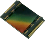
A Charge Coupled Device (CCD) is a highly sensitive photon detector. The CCD
is divided up into a large number of light-sensitive small areas (known as
pixels) which can be used to build up an image of the scene of interest. A
photon of light which falls within the area defined by one of the pixels will be
converted into one (or more) electrons and the number of electrons collected
will be directly proportional to the intensity of the scene at each pixel. When
the CCD is clocked out, the number of electrons in each pixel are measured and
the scene can be reconstructed.
The picture here shows a "typical" CCD. The CCD itself is primarily made of
silicon and the structure has been altered so that some of the silicon atoms
have been replaced with impurity atoms.
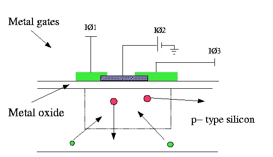
The figure below shows a very simplified cross section through a CCD. It can
be seen that the Silicon itself is not arranged to form individual pixels. In
fact, the pixels are defined by the position of electrodes above the CCD itself.
If a positive voltage is applied to the electrode, then this positive potential
will attract all of the negatively charged electrons close to the area under the
electrode. In addition, any positively charged holes will be repulsed from the
area around the electrode. Consequently a "potential well" will form in which
all the electrons produced by incoming photons will be stored.
As more and more light falls onto the CCD, then the potential well
surrounding this electrode will attract more and more electrons until the
potential well is full (the amount of electrons that can be stored under a pixel
is known as the full well capacity). To prevent this happening the light must be
prevented from falling onto the CCD for example, by using a shutter as in a
camera. Thus, an image can be made of an object by opening the shutter, "integrating"
for a length of time to fill up most of the electrons in the potential well, and
then closing the shutter to ensure that the full well capacity is not exceeded.
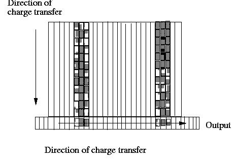
An actual CCD will consist of a large number of pixels (i.e, potential wells),
arranged horizontally in rows and vertically in columns. The number of rows and
columns defines the CCD size, typical sizes are 1024 pixels high by 1024 pixels
wide. The resolution of the CCD is defined by the size of the pixels, also by
their separation (the pixel pitch). In most astronomical CCDs the pixels are
touching each other and so the CCD resolution will be defined by the pixel size,
typically 10-20µm. Thus, a 1024x1024 sized CCD would have a physical area image
size of about 10mm x 10mm.
How is a CCD clocked out ?
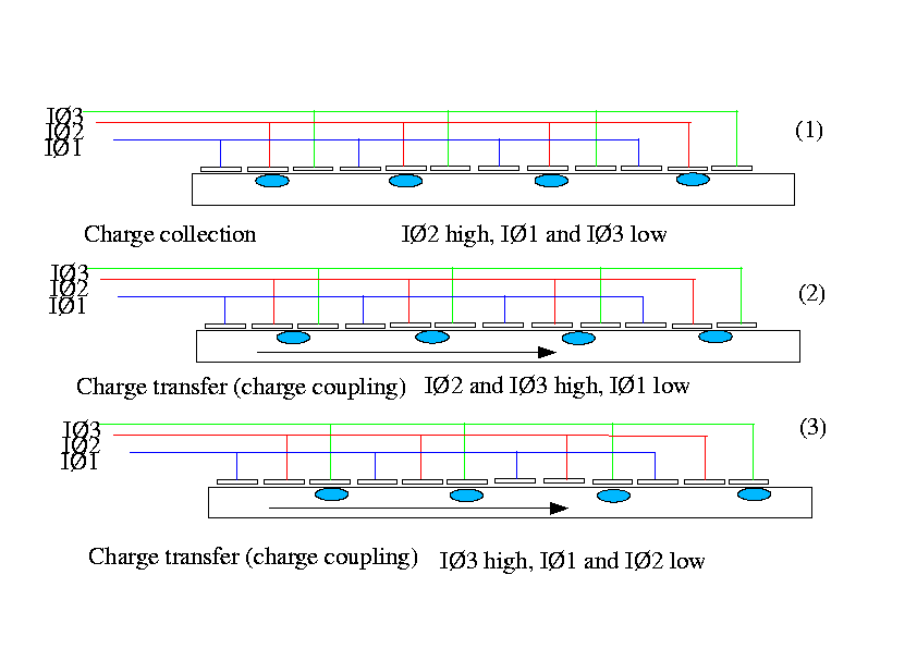
The figure below shows a cross section through a row of a CCD. Each pixel
actually consists of three electrodes IØ1, IØ2, and IØ3. Only one of these
electrodes is required to create the potential well, but other electrodes are
required to transfer the charge out of the CCD. The upper section of the figure
(section 1) shows charge being collected under one of the electrodes. To
transfer the charge out of the CCD, a new potential well can be created by
holding IØ3 high, the charge is now shared between IØ2 and IØ3 (section 2). If
IØ2 is now taken low, the charge will be fully transferred under electrode IØ3 (section
3). To continue clocking out the CCD, taking IØ1 high and then taking IØ3 low
will ensure that the charge cloud now drifts across under the IØ1 electrodes. As
this process is continued, the charge cloud will progress either down the
column, or across the row, depending upon the orientation of the electrodes.
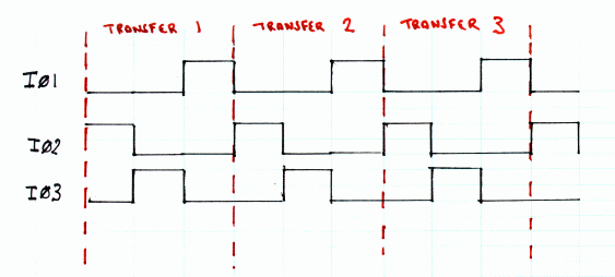
The figure below (called a clocking diagram) shows the progression under
which each electrode is held high and low to ensure that charge is transferred
through the CCD.
Initially, IØ2 is high - usually to around 12V, and the charge is held under
that electrode as in (1) previously. When IØ3 is held high, and IØ2 is taken low
(usually 0 V), the charge migrates under the IØ3 electrode (as in (2)). Finally,
taking IØ1 high and IØ3 low transfers the charge under IØ1 (as in (3)). This
process is repeated in transfer 2 and transfer 3, the charge has now been moved
three pixels along. This process is known as charge coupling (hence CCD).
For most of the CCD, the electrodes in each pixel are arranged so that the
charge is transferred downwards along the columns. Hence, during the CCD
clocking operation, rows are transferred downwards to the final row (the readout
register) which is used to transfer the charge in each pixel out of the CCD so
it can be measured.
In the read out register, the electrodes are arranged so that the charge is
transferred in the horizontal direction, along the readout register.
How the charge is measured
The final process on the CCD is the reading of each pixel so that the size of
the associated charge cloud can be measured. At the end of the readout register
is an amplifier which measure the value of each charge cloud and converts it
into a voltage, a typical conversion factor being around 5-10µV per electron
with "typical" full well values being about 100,000 electrons or so.
A CCD camera will consist of the CCD chip, and associated electronics, which
is used at this point to amplify the small voltage on the CCD, remove noise
components, digitise the pixel values and output the values of each pixel for
example, to a PC, where the image can be processed in software and the image
displayed. The CCD is an analogue device, and the analogue voltage values are
converted into a digital form by the camera electronics.
Not every photon falling onto a detector will actually be detected and
converted into an electrical impulse. The percentage of photons that are
actually detected is known as the Quantum Efficiency (QE). For example, the
human eye only has a QE of about 20%, photographic film has a QE of around 10%,
and the best CCDs can achieve a QE of over 80%. Quantum efficiency will vary
with wavelength.
Wavelength range
CCDs can have a wide wavelength range ranging from
about 400nm (blue) to about 1050nm (Infra-red) with a peak sensitivity at around
700nm. However, using a process known as backthinning, it is possible to extend
the wavelength range of a CCD down into shorter wavelengths such as the Extreme
Ultraviolet and X-ray.
Dynamic Range
The ability to view bright and faint sources correctly in the same image is a
very useful property of a detector. The difference between a brightest possible
source and the faintest possible source that the detector can accurately see in
the same image is known as the dynamic range. When light falls onto a CCD the
photons are converted into electrons. Consequently, the dynamic range of a CCD
is usually discussed in terms of the minimum and maximum number of electrons
that can be imaged. As more light falls onto the CCD, more and more electrons
are collected in a potential well, and eventually no more electrons can be
accommodated within the potential well and the pixel is said to be saturated.
For a typical scientific CCD this may occur at around 150,000 electrons or so.
The minimum signal that can be detected is not necessarily one electron
(corresponding to one photon at visible wavelengths). In fact, there is a
minimum amount of electronic noise which is associated with the physical
structure of the CCD and is usually around 2-4 electrons for each pixel. Thus,
the minimum signal that can be detected is determined by this readout noise.
In the example above, the CCD would have a dynamic range of 150,000:4 (taking
the upper noise level). But - this dynamic range is also dependent on the
ability of the electronics to be able fully digitise all of this dynamic range (see
the more detailed CCD information for discussions on electronics resolution).
Linearity
On the whole, the eye is not a linear detector (except over very small
variations in intensity) and has a logarithmic response. An important
consideration in a detector is its ability to respond linearly to any image it
views. By this we mean that if it detects 100 photons it will convert these to
100 electrons (if we had 100% QE) and if it detects 10000 photons, it will
convert these to 10000 electrons. In such a situation, we say that the detector
has a linear response. Such a response is obviously very useful as there is no
need for any additional processing on the image to determine the 'true'
intensity of different objects in an image.
Noise
One of the most important aspects of CCD performance is its noise response.
There are a number of contributions to the noise performance of a CCD, these are
briefly listed here:
Dark current - i.e thermally generated noise. At room temperature, the
noise performance of a CCD can be as much as thousands of electrons per pixel
per second. Consequently, the full well capacity of each pixel will be reached
in a few seconds and the CCD will be saturated. Dark current can be massively
reduced by cooling. For example, the noise performance of the CCD could be
reduced from thousands of electrons at room temperature to only tens of
electrons per pixel per second at -40 degrees C. By cooling down to
temperatures below about -70 degrees C dark current can be virtually
eliminated (substantially below one electron per pixel per second). A second
way of reducing noise is to slightly alter the CCD processing technique to
produce a Multi-Pinned -Phase (MPP) CCD. This technique can reduce the dark
current to very low levels (a few hundred electrons per pixel per second at
room temperature).
Readout noise - the ultimate noise limit of the CCD is the readout noise.
The readout noise originates from the conversion of the electrons in each
pixel to a voltage on the CCD output node (a typical value would be around 4µV
per electron). The magnitude of this noise depends on the size of the output
node. A large amount of effort has been dedicated to reducing the CCD readout
noise, as this noise value will ultimately determine the dynamic range and
should be as low as possible, particularly when detecting very faint sources
for example, detecting photons at X ray energies such as in the XMM-Newton
mission. Noise values of 2-3 electrons rms (root mean square) are now typical
for many CCDs but some companies have recently claimed a noise resolution of
under 1 electron rms.
When the CCD is used as part of a camera for astronomical imaging, other sources
of noise must also be included such as the random (shot) noise present on the
image itself, along with noise introduced by the camera electronics. However,
these noise sources are discussed elsewhere.
Power
CCDs themselves consume very little power. During
integration, only a very small current is flowing and the CCD consumes only 50mW
or so. Whilst the CCD is being clocked out more power can be consumed but this
is typically only several Watts or so. Of course, the electronics required to
operate the CCD and process images can consume much more power.
Why are scientific CCDs so expensive ?
A Video camera using a CCD can be bought for as little as 400-500 pounds.
However, a scientific grade CCD may cost up to 100 times this price, sometimes
more. Some of the reasons why scientific CCDs are much more expensive than CCDs
in consumer electronics are outlined below:
Cost and complexity
Scientific grade CCDs are much more expensive than the basic type of CCDs
that are usually found in devices such as commercially available Video cameras.
Commercially available video cameras normally have a number of disadvantages
that make them unsuitable for scientific use. For example:
Commercial CCDs may contain a larger number of defects and blemishes which
will degrade the image quality. For the sort of images usually viewed by a
video camera these blemishes are not a problem as they can be removed by
software in the camera. For scientific use however, the image quality would be
unacceptably degraded;
The noise of commercial CCDs and their camera systems is much higher than
for specially built scientific systems;
The dynamic range of the camera system is much lower than for scientific
cameras.
When a CCD image is taken, noise will appear as well as the main CCD image.
Noise can be thought of as unwanted signal which doesn't improve the quality of
the image. In fact, it will degrade it. The main problem with noise is that most
noise is essentially random, and so cannot be completely removed from the image.
For example, if we know that a noise source contributes 10 units on each image
we can subtract those 10 units from the image. If we only know that the noise is
'around' 10 units, then we can't completely remove all of this noise (as we don't
know its exact value).
The main contributions to CCD noise are:
Noise on the image itself ("shot noise")
The detection of photons by the CCD is a statistical process. If images are
taken over several (equal) time periods, then the intensity (the number of
photons recorded) will not be the same for each image but will vary slightly. If
enough images are taken, it will be seen that the deviation in intensity found
for each image follows the well known Poisson distribution. In effect, we
cannot be sure that the intensity we have measured in a particular image
represents the "true" intensity as we know that this value will deviate from the
average. It is this deviation which is considered to be the noise associated
with the image. As the deviation is known to follow a Poisson distribution, we
know that the likely deviation will be plus or minus the square root of the
signal intensity measured. Thus, if we measure a signal intensity of one hundred
photons, then the noise on this signal will be ten photons. If we measure a
signal intensity of one thousand photons in the image, then the noise on this
signal will be about thirty one photons.
Thermally generated noise:
Additional electrons will be generated within the CCD not by the absorption of
photons (i.e the signal) but by physical processes within the CCD itself. The
number of electrons generated in a second will be dependent on the operating
temperature of the CCD and hence this noise is known as thermal noise (sometimes
also known as dark noise). As with the detection of the signal, the same number
of electrons will not be generated in equivalent periods of time as the thermal
noise will also have a Poisson distribution.
Other noise contributions also affect image quality. A very good description
of how noise can affect the quality of CCD images can be found on the
Sky and Telescope
CCD imaging pages.
Some of the Physics behind the generation of various types of noise within a
CCD are explained below.
Some Physical Principles behind CCD noise
Dark current
Even in the absence of light, thermally generated electrons will be collected
in the CCD and will contribute to the overall signal measured. There are three
main contributions to dark current:
thermal generation at surface states;
thermal generation within the bulk silicon;
thermal generation in the depletion region.
The vast majority of the thermally generated electrons are generated at the
surface states. Interface states can exist in the forbidden energy gap between
the valence and conduction bands (such states do not exist in a perfect lattice
and are caused by the change in energy within the lattice due to the
introduction of an impurity atom or lattice defect). An electron can be excited
by absorption of a phonon with insufficient energy to excite the electron into
the conduction band but with sufficient energy to excite it into the mid-band
interface state. A second phonon can then excite the electron into the
conduction band.
However, if the interface states are filled up by free carriers then the dark
current will be drastically reduced. Such a process can be achieved by operating
the CCD in inversion which is a technique used by all modern CCDs. When the CCD
is operated in inverted mode, holes from the channel stops migrate to fill the
interface states. Two of the three electrodes defining a pixel are driven into
inversion to drastically reduce the dark current (it is not possible to invert
all three electrodes as a potential well is still required to collect charge).
If a CCD is not inverted, then the dark current generation rate may be as high
as several hundreds of thousands of electrons per pixel per second (at room
temperature) whereas an inverted CCD will have a much lower generation rate of
about ten thousand electrons per pixel per second.
If such a CCD is read out a number of times per second (for example in a
video camera) then the dark current at room temperature is low enough not to
significantly interfere with image quality. However, if the CCD is only read out
once a second (or less frequently) then the number of thermally generated
electrons will be to high for adequate image quality. Hence, additional measures
need to be taken.
The simplest way to reduce the dark current is to cool the CCD as dark
current generation is temperature related.
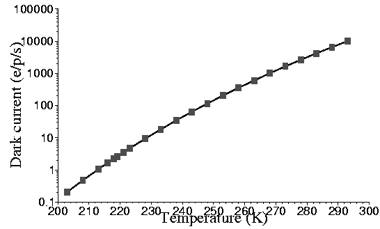
The figure below shows the variation in dark current with temperature for a
CCD with a room temperature dark current of 10,000 electrons/pixel/s. There are
a number of ways in which a CCD can be cooled, the easiest is to use liquid
Nitrogen but thermoelectric coolers (Peltier coolers) can be used, and in space
the CCD can be cooled with a direct connection to a passive radiator.
A second way of reducing the dark noise in a CCD is to use a Multi-Pinned
Phase (MPP) device. In an MPP device, it is possible to operate the CCD with all
three electrode phases driven into inversion. This is accomplished by adding a
suitable dopant under one of the phases during CCD fabrication. The presence of
the additional dopant under one of the phases alters the potential under that
phase so that there is still a potential well present during integration when
all the electrode phases are at clock low level (usually zero volts). Dark
current is now only generated in the bulk silicon reducing the dark current to
about 300 electrons/pixel/signal.
Readout noise
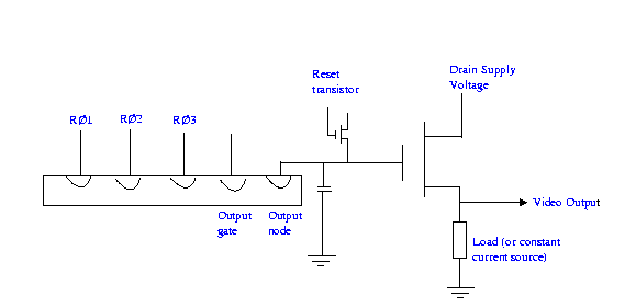
The ultimate noise limit of the CCD is determined by the readout noise. The
readout noise is the noise of the on-chip amplifier which converts the charge (i.e
the electrons) into a change in analogue voltage using:
Q= CV where Q is the charge on the output node, and C is the output node
capacitance. V is the voltage sensed by the on-chip amplifier operating as a
source follower.
The figure above shows a schematic of a typical CCD output section. The
charge in a pixel is transferred onto the output node where the change in
voltage caused by this charge is sensed by the on-chip amplifier.
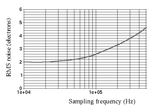
The on-chip amplifier will have an associated noise performance which is
typically 1/f at low sampling frequencies with a white noise floor at higher
sampling frequencies. The sampling frequency corresponds to the rate at which
each pixel is read by the CCD.
The figure above shows the readout noise response versus the sampling
frequency for a typical CCD. It can be seen that as the sampling frequency
increases, the root mean square value of the read out noise increases.
 chema
più usato consiste nel dipingere i pixel adiacenti secondo lo schema GRGB
Green (verde), Red (rosso), Blue (blu), Green (verde) (si noti che il verde
è il colore a cui l’occhio umano percepisce la maggior parte di dettagli). I
colori appena citati sono i colori primari, da questi è possibile ottenere
qualsiasi altro colore.
chema
più usato consiste nel dipingere i pixel adiacenti secondo lo schema GRGB
Green (verde), Red (rosso), Blue (blu), Green (verde) (si noti che il verde
è il colore a cui l’occhio umano percepisce la maggior parte di dettagli). I
colori appena citati sono i colori primari, da questi è possibile ottenere
qualsiasi altro colore.