OK, this is a little tricky, and it requires some expertise,
but if you darebeing bold it will give you a lot of satisfaction
as it did to me a few years ago.
At the time I owned a TRS80-100 with 8K ram and did not want
to spend the money to buy the original chips for the memory upgrade.
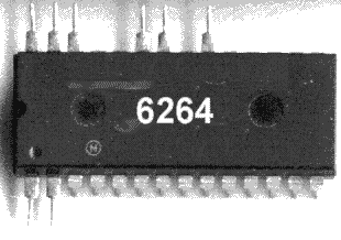
On the other hand I had several 6264LP
in my lab, and I decided to use them up. (LP stands for LowPower!)
I just found the schematics, and you have to forgive me if
you'll have to fill in the blanks, but I am myself trying to
put it all back together as I write.
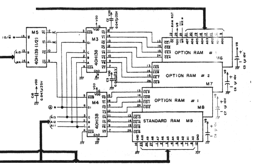
To begin, the TRS80-100 should have 3 empty sockets for the
original chips.
Each original chip had 4 2K Static Ram modules that are enabled
by CE1.CE2.CE3.CE4 for a
total of 8K.
The 3 sockets are connected pin by pin, except for the CE
pins that obviously come from different outputs of the memory
decoder.
The yellow pinout represents each socket as it is on the
M-100.
Because the 6264LP chip is a single 8K bank, it does not
require 4 separate chip select, but just one (CS1), while CS2
is used to put the chip into stand by mode.
Most of the pins between the socket and the 6264LP are compatible,
but not all.
NC
6264LP
VCC
A12
WE
A7
A7
1
Socket
28
VB
CS2
A6
A6
A8
A8
A5
A5
A9
A9
A4
A4
>>
WE
A11
A3
A3
>>
CE4
OE
A2
A2
A10
A10
A1
A1
>>
OE
CS1
A0
A0
D7
D7
D0
D0
D6
D6
D1
D1
D5
D5
D2
D2
D4
D4
GND
GND
D3
D3
CE1
GND
CE2
14
15
CE3
It is first necessary to "open out" the "incompatible"
pins of the 6264LP. With this I mean, bend those pins 90 degrees
so that they "stick out" instead of being parallel
to the other ones. The procedure is simple and harmless to the
chip if done just once.
Now the chip can be inserted in the socket
To reach the full 32K capacity, 3 chips 6264LP should be
mounted: one for each socket. Now we need to complete the connections.
A11 and A12 need to be wired to each 6264LP from the motherboard;
best shot is to do it from M3 or M4 (40H138 pins 1 & 2).
So use very thin insulated wire (like the type use for wire wrapping)
to connect the following:
6264LP
Board
23 (A11)
M3 1
2 (A12)
M3 2
27 (WR)
Socket 25 (WE)
22 (OE)
Socket 22 (RamRst)
28 (VCC)
Socket 28 (VB)
26 (CS2)
M3 16 (VDD)
At last, we need to install the "new" memory address
decoder, a 74HC138 or 40H138 to provide the CS1 to each 6264LP.
For convenience, you can solder it "on top" of M3 or
M4 by opening up all pins except for 8 and 16 which will connect
to the power directly from the chip below.
Signals A13,A14, and A15 can be wired from the system bus
connector or from M16/M17.
Because the standard RAM is located at the top of the 64K,
it "would" be activated when Y7 becomes active (low).
We don't need to use this signal because the standard Ram is
already addressed and enabled on the mother board. On the other
hand, we'll use Y6, Y5 and Y4 to enable the 3 additional chips
(or less) that we have added.
BOARD
HC138
BOARD
A13
A0
1
16
VCC
VDD
A14
A1
2
15
Y0
A15
A2
3
14
Y1
GND
G2A
4
13
Y2
GND
G2B
5
12
Y3
VDD
G1
6
11
Y4
to CS1-1
Y7
7
10
Y5
to CS1-2
GND
GND
8
9
Y6
to CS1-3
Conclusion
I have built this myself a few years ago and had no trouble
with the computer since. I recommend to take out all batteries,
turn off the memory backup battery, and use a small power grounded
soldering tool for the wiring. Unfortunatelly, I have sold the
unit that was modified, and I don't have a picture of what it
looks like after the "surgery".
Good luck, and feel free to Email
me for any help I can give you about this project.