![]()
I have evaluated the performances of power supply blocks with PSpice simulations on 2 levels of detail.
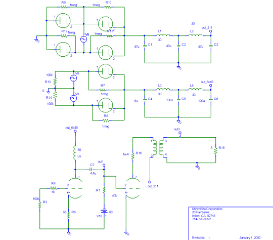
Fig. 1 The schematic used in the 1st level of power supplies simulation
In the schematic of Fig.1, the ac supply voltages has been introduced abruptly. This condition was purposely introduced in order to run a worst-case simulation set. The 1Mohm Resistor in parallel with diodes was deliberately introduced for Spice convergence improvement. The results are summarized in Figg. 2-7.
In Fig. 2, harmful bumps exhist during the first 400ms after turn-on. The huge presence of magnetic components inside this amp produce in this time-frame, voltage overshoots as response to the enourmous request of current by vacuum devices and power supply capacitors at turn-on. The LC coupling between the driver and the 211 stage, transfers a bit of the overshoots to the driver power supply. This voltage bump overcomes the DC negative biasing of 211 grid producing a positive voltage into the same grid (vout3 in Fig.3). As a result you have an harmuful plate dissipation in the output tube (Fig. 4) derivated by the contemporanery presence of high plate voltage and positive grid voltage.

Fig.2
Steady-state voltage are a bit higher of real values due to the adsence of parasitcs resistor inside the magnetics.
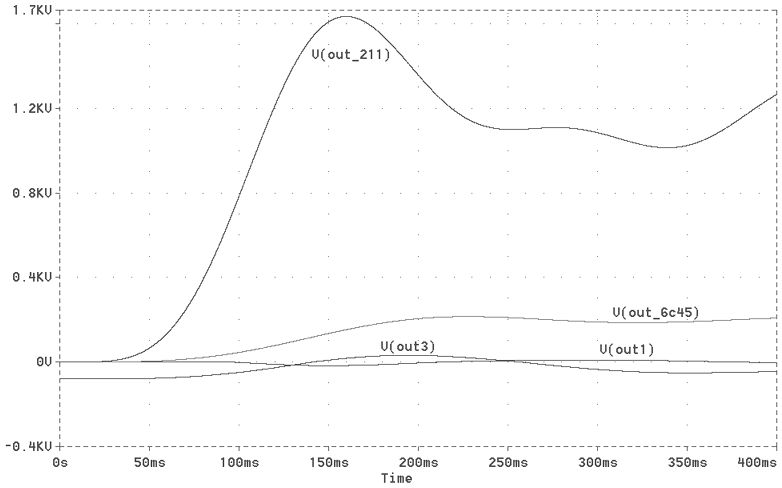
Fig. 3
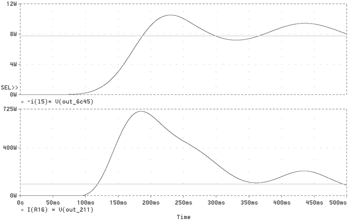
Fig. 4 The dynamic power dissipation on 6C45 and 211 plates

Fig. 5 Diode pulse currents at start-up
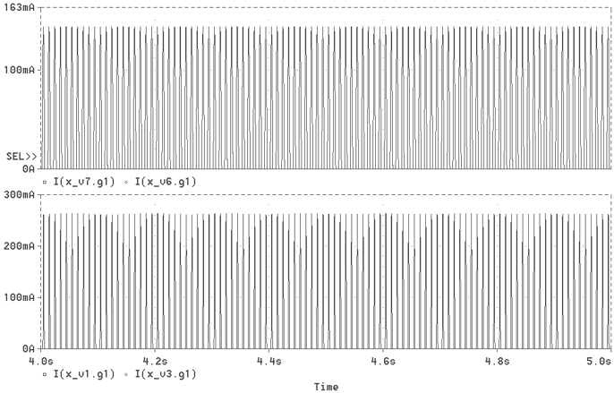
Fig. 6 Repetitive diodes peak current
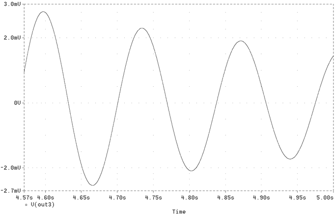
Fig. 7 Residual hum at the output pin after 4s from start-up
This effects can be mitigated strongly using the inherent property of vacuum devices of warm-up time, i.e. the requested for the cathode heating (and the subsequent nominal production of electrons). This is the raison of the presence in the power supply schematic of a monitor circuitry devoted to relais driving.
The monitor behave as follows:
After the switching of HS the 211 cathode, the 6c45 heater, the grid voltage power supply and the monitor circuit are activated;
After a time requested to stabilize this voltages (time t1), the monitor drive on the M1 wire producing the activation of vacuum diode heaters by the closing of RE1..RE10 contacts ;
At the time t2, after that bouncing on relais are terminated, the monitor drive on the M2 wire produncing in this way the activation of the HV rails by the closing of RE11, RE12 contacts. .
Clearly the time difference t2-t1 must be evaluated attentively since we must guarantee a danger free switching (i.e. without the presence of high voltages) of contacts drived by M1 (that requires a t2-t1 difference high) but on the other side the relais driven by M2 must be closed when vacuum diode cathode are still cold otherwise we cannot reduce the initial overvoltages and output plate dissipation. Depening on the chosen relais this times difference could be between 20 and 300ms.

Fig 8 The schematic used in the 2nd level of power supplies simulation
The schematic of Fig. 8 adds behavioural blocks in order to simulate the effect of a cold start with the control of the monitor circuitry. The graphic in Fig. 9 summarizes 10 seconds of simulation after the turning on of the main switch. No overshootes are shown, the 211 supply voltage raise gently and grid voltage is always in the negative range. Therefere the dynamic plate dissipation is not dangerous both for the 6c45 and 211 tubes. This results are mirrored also but the beheviour of repetitive pulse current produced by the vacuum diodes. No surges are shown at the start-up and the envelopes raise softly, Fig. 11.
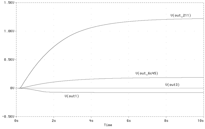
Fig 9
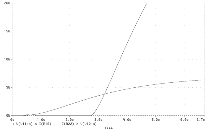
Fig 10
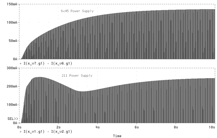
Fig. 11
A great deal of attention was reserved also to the simulation of the amplifier block. For the performances in terms of square-wave response I have used the schematic in Fig. 12.
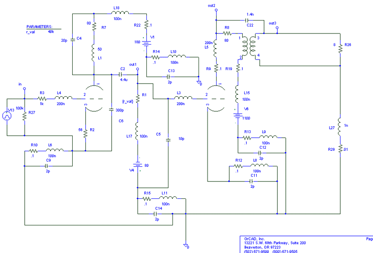
Fig. 12 The simulated amlifier block for the square-wave response evaluation
This schematic is based in a worst case evaluation of main parasitc elements involved in the amplification process. RLC block take in count parasitcs of the connections on supply rails, ground bus and devices used for the amplifier building.Clearly the values are depending strongly by the quality of wiring.
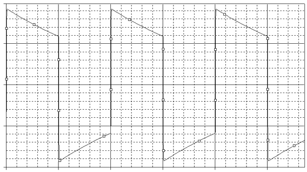
Fig.13 The 100Hz Sqaure Wave Output
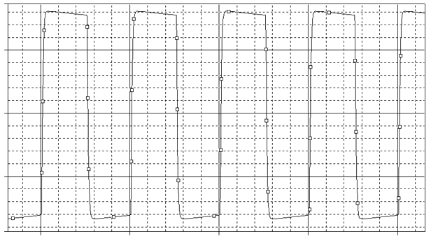
Fig.14 The 1kHz Square Wave Output
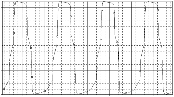
Fig.15 The 10kHz Square Wave Output
Solid State designers can be a bit amazed about this poor electric response but Vacuum Tube based ones know that this performances can be considered good particularly if we think that this results refer to the full output power. However as known, the main limiting factor for a SE triode amplifier is the output transformer.
For the evaluation of other parameter I have particularized again the schematic of Fig.12 by the introduction of a simple passive model for the loudspeaker that replace the output resistor, Fig.16 and Fig.17.
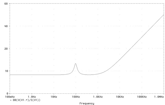
Fig.16 Impedance response for the loudspeaker model
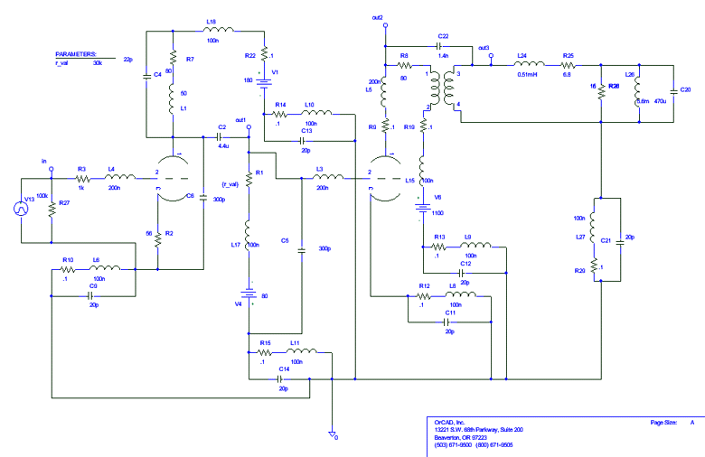
Fig. 17 The simulated amplifier block including the loadspeaker model
The first consequence deriving by loudspeaker model introduction is a worsening in terms of linear distortion with respect to resistor load case, Fig. 19
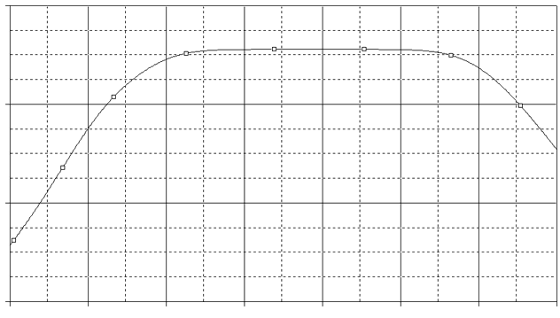
Fig. 18 Frequency Response with resistor load
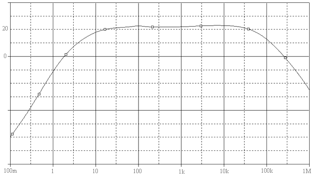
Fig. 19 Frequency Response with loadspeaker
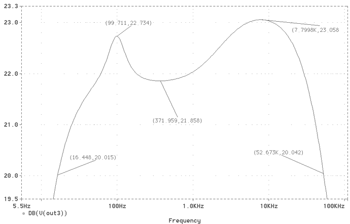
Fig. 20 Frequency Response with loadspeaker detail
The Zoom of Fig. 20 shows in depth this harmful mechanism however kept within 1dB.
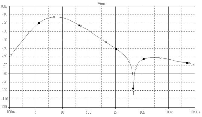
Fig. 21 The Output Power Supply Rejection Ratio (Driver Stage injection)
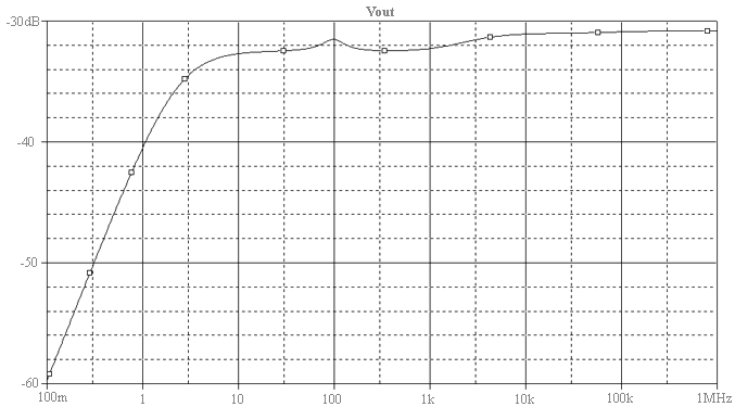
Fig. 22 The Output Power Supply Rejection Ratio (Output Stage injection)
Depending by Loadspeaker characteristic we have different performances in terms of output power and THD. In general a rise in the load impedance produces a lower output power with a lower THD and mutatis mutandis to low loads correspond more power and higher THD. This behaviour is perfectly mapped in this amplifier as Figg. 23-28 show.
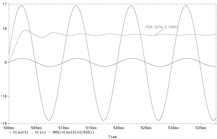
Fig. 23 The 100Hz Output Sinusoidal wave in union with the Output Power
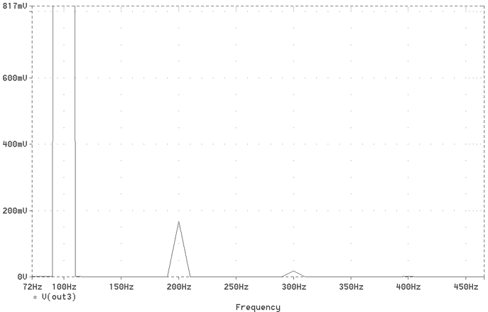
Fig. 24 The 100Hz THD
| HARMONIC FREQUENCY FOURIER NORMALIZED PHASE NORMALIZED NO (HZ) COMPONENT COMPONENT (DEG) PHASE (DEG) 1 1.000E+02 1.697E+01 1.000E+00 8.210E+00 0.000E+00 2 2.000E+02 1.680E-01 9.903E-03 9.910E+01 9.089E+01 3 3.000E+02 1.763E-02 1.039E-03 1.302E+01 4.806E+00 4 4.000E+02 1.708E-03 1.007E-04 -6.306E+01 -7.127E+01 5 5.000E+02 5.403E-05 3.184E-06 1.532E+02 1.450E+02 TOTAL HARMONIC DISTORTION = 9.958287E-01 PERCENT |
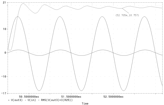
Fig. 25 The 1kHz Output Sinusoidal wave in union with the Output Power
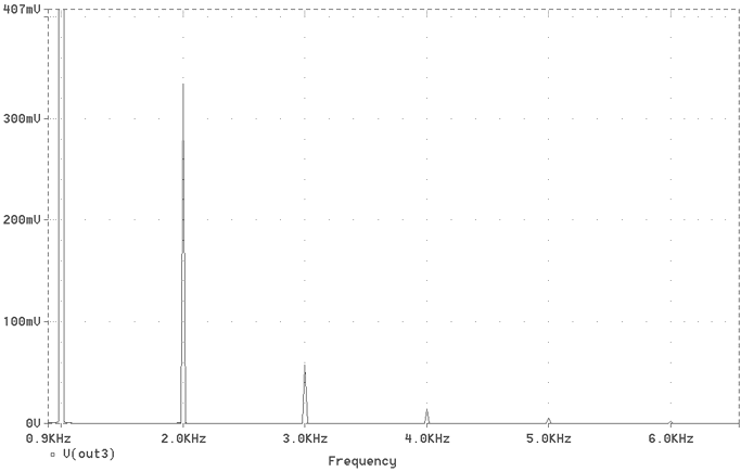
Fig. 26 The 1kHz THD

Fig. 27 The Lissajous Plot for the 1kHz signal
| HARMONIC FREQUENCY FOURIER NORMALIZED PHASE NORMALIZED NO (HZ) COMPONENT COMPONENT (DEG) PHASE (DEG) 1 1.000E+03 1.567E+01 1.000E+00 3.555E+00 0.000E+00 2 2.000E+03 3.325E-01 2.122E-02 7.195E+01 6.839E+01 3 3.000E+03 5.669E-02 3.617E-03 -3.507E+01 -3.862E+01 4 4.000E+03 1.400E-02 8.930E-04 -1.513E+02 -1.548E+02 5 5.000E+03 4.896E-03 3.124E-04 9.561E+01 9.205E+01 TOTAL HARMONIC DISTORTION = 2.154191E+00 PERCENT |
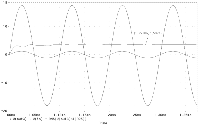
Fig. 28 The 10kHz Output Sinusoidal wave in union with the Output Power
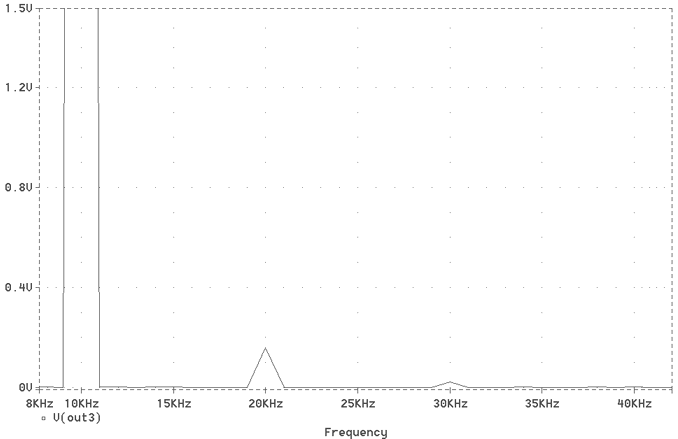
Fig. 29 The 10kHz THD
| HARMONIC FREQUENCY FOURIER NORMALIZED PHASE NORMALIZED NO (HZ) COMPONENT COMPONENT (DEG) PHASE (DEG) 1 1.000E+04 1.783E+01 1.000E+00 -1.601E+00 0.000E+00 2 2.000E+04 1.579E-01 8.859E-03 7.546E+01 7.706E+01 3 3.000E+04 2.009E-02 1.127E-03 -1.628E+01 -1.468E+01 4 4.000E+04 2.295E-03 1.287E-04 -1.138E+02 -1.122E+02 5 5.000E+04 3.067E-04 1.720E-05 1.548E+02 1.564E+02 TOTAL HARMONIC DISTORTION = 8.931411E-01 PERCENT |
|
What did you
think of this article? |