
Tab.1 - TMS4C2972/3 Test modes list.
I- Description of the chip
Tab.1 - TMS4C2972/3 Test modes list.
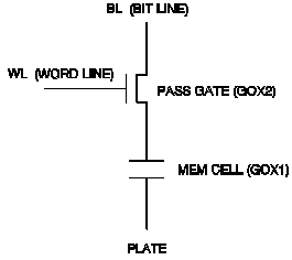
TMS4C2972/3 is a 2.9 megabit serial memory based on 0.5 micron DRAM trench array. The chip has 36 pins: 2 for VDD, 2 for VSS, 12 for data inputs D0-D11, 4 for input controls (RSTW = Reset Write, SWCK = Serial Write Clock, WE = Write Enable, IE = Input Enable), 12 for data outputs Q0-Q11, 4 for output control (RSTR = Reset Read, SRCK = Serial Read Clock, RE = Read Enable, OE = Output Enable). TMS4C2973 low voltage version is operated at VDD = 3.4V nominal, and power supplies VARY for the array and VPERI for periphery are directly connected to VDD. TMS4C2972 high voltage version is operated at VDD = 5V nominal and VARY,VPERI are internally generated to have internal supply at 3.4V anyway. All other relevant voltages are internally generated by charge pumps or regulators: VPP to overdrive n channel pass gate to select trench cell; BLR (Bit Lines Reference) to equalize Bit Lines before sensing; VPLT (Plate Voltage) to give reference to the common terminal of trenches (Fig.1). Data are serially written and read under external signals control while an arbiter,clocked by internal oscillator, manages self refresh and parallel tranfer of group of 40 data into the array.
Test modes are entered mantaining RSTW and WE high for more than 1024
SWCK with no need of high voltage detection. In the specs is clearly said
that is not allowed to mantain RSTW and WE high for more than 1024 SWCK
if a normal operation is desired. Test codes are on inputs DIN3,DIN2,DIN1,DIN0.
All test modes are concurrent. There is a special code ( NO TEST ANYMORE
) to stop code entry and another special code ( EXIT ALL TEST MODES ) to
reset all test functions entered. Test modes list is reported in tab.1.
Test modes 1-5 are mainly designed to electrically stress the chip to reduce
or avoid burn-in. Using combinations of these test modes is possible to
stress periphery and array (especially GOX1 and GOX2) of the chip, leading
to a screening which is equivalent to traditional burn-in. Evaluations
of the possibility to use DFT stress instead traditional burn-in have been
done with positive results in KTI, TECH and AMOS on 4meg Hydra. Test modes
6-7 allow to know if a defective unit has been repaired using redundancy.
Test 8 allows to do pause test stopping the internal refresh operation.
Test 9 is designed to force internal oscillator thus controlling the base
frequency of the arbiter. Tests 10-11 allow to monitor process dependency
of some critical digital and analog internal signals. Tests 12-13 are designed
to be sure that chip is operating under a particular test mode and there
is no inadvertent test mode exit due to noise or to high vales of power
supply or temperature.
Test modes that require to force outputs are designed to not impact
speed path and test information is treated as data before the last clocked
flip-flop of the read chain.
ANALOG MONITOR test that require to force analog voltages to TTL input
pads are designed to avoid TTL detect to work in current trough area. TLMON
control signal disables the TTL detect circuits.
1) enable entry by RSTW=WE=high for more than 1024 SWCK;
2) enter codes of desired test modes;
3) enter TLNTA test mode;
4) exercise the chip in the enterd test modes without risk to enter
undesired new test modes;

Fig.2 : DFT Control Block Schematic.
4) enable entry by RSTW=WE=high for more than 1024 SWCK and enter TLCLR test mode when we want to exit testing session. Waveforms associated with suggested entry-exit sequence are reported in Fig.3 and Fig.4.
In VPP TO VDD test the voltage VPP is connected to VDD.

Fig.3 : DFT Entry Sequence.
WORD LINE STRESS test consists of the following actions: all the word lines are enabled at the same time; all the redundant word lines are enabled at the same time; activity of all sense amplifiers is stopped and they are equalized to bit line reference voltage (BLR); BLR, usually set at VARY/2 to allow sense swing starting from mid point, is now set to VSS. The purpose of this test mode is to induce maximum stress across pass gates channel in all the array at the same time. Contemporary enabling of all word lines is basically obtained forcing high all the row address (RA) and all their inverses (RA_) thus enabling all row factor signals (RF) after the row address decoders. Contemporary enabling of all redundant word lines is basically obtained directly enabling redundant row factors after row redundancy fuses decoders. Sense amplifiers activity stop and their equalization is obtained by forcing off timing chain that fires different phases of sensing operation. BLR=VSS is directly obtained at the BLR generator disabling the partition circuit designed to obtain BLR=VARY/2 and connecting BLR directly to VSS. During word line stress, VPP pump is overloaded by contemporary enabling of all word lines; Vpp voltage has a drop and it is necessary a long period of time to allow pump recover. If VPP TO VDD test is also entered, the time necessary to have VPP at steady state is reduced to 15 microseconds.
Top plate voltage is usually at VARY/2 to allow a simmetrical behaviour of the storage cell when we want to write 0 or 1 and to reduce voltage stress across the storage cell mantaining maximum swing across the cell at VARY/2 value. TOP PLATE HIGH and TOP PLATE LOW are two test modes that allow to vary the top plate voltage clamping it at VARY and VSS rispectively. They allow to stress the accessed storage gate oxide when 0 or 1 are respecti- vely written in the storage node. In TOP PLATE HIGH test, the stress across the storage cell can be greatily accelerate using WL STRESS also. In TOP PLATE LOW test, the stress across the storage cell is enhanced using CHIP STRESS also. TOP PLATE HIGH and TOP PLATE LOW are mutually exclusive in the sense that if TOP PLATE LOW is entered, TOP PLATE HIGH is reset and viceversa.
For failure analysis purpose it is often useful to know if a chip has been repaired using redundancy. This is useful particularly when chip is packed and there is no possibility to look at fuses using a microscope.The two test modes ROW REDUN CALL and COL REDUN CALL have been designed for this purpose. When ROW REDUN CALL test is entered, a comparison between row redundancy fuses and address of the accessed row is activated and, if they match, output Q7 is forced high otherwise is forced low. In TMS4C2972/3 field memory, array access is managed by an arbiter on demand of a pheriphery counting logic and duration of this access is 100 nsec based on internal fixed frequency clock. As a consequence of this organization, array access will happen within 40 external clocks starting from the pheriphery request but it is not known from external when exactly it will happen. In the ROW REDUN CALL test circuits there is a flip-flop to latch the result of row address and row fuses matching in write mode in order to be sure to catch that information even if very long external clocks are used compared to 100 nsec. When COL REDUN CALL test is entered, a comparison between column redundancy fuses and address of the selected column is activated and, if they match, output Q7 is forced high otherwise is forced low. For COL REDUN CALL test there is not the latching system of ROW REDUN CALL because the match between column fuses and column address is done before array is accessed and is syncronous with external clock.
REFRESH OFF test mode allow to stop internally controlled refresh operations. In this way is possible to perform pause test and evaluate how long is data retention of memory cells. Pause test is performed according to the following steps: 1) REFRESH OFF test mode is entered followed by NO TEST ANYMORE; 2) starting from a RSTW pulse, memory is completely written at a minimum cycle time using all 1 (or other patterns if a pattern sensitivity is under evaluation). This write operation will take little bit longer than 6 msec; 3) tester does not perform any write or read operation for a time T; 4) chip is completely read at a minimum cycle time starting from a RSTR pulse. If it doesn't fail, the read operation is repeated using a wait time longer than T. The maximum T value for wich the chip doesn't fail is the data retention.
INT OSC FORCED is a test mode that allows SWCK to be a clock for the arbiter instead of the internal oscillator clock. Furthermore in this test mode SWCK is taken before it is gated by WE having in this way the possibily to stop write operation while having arbiter running. This test mode is useful in the debug phase of the chip if we want to stop or start the arbiter at a given frequency and have it syncronized with an external signal.
INT OSC MONITOR is a test mode that allows to read on output Q8 a signal derived from the internal oscillator. The signal that will be read from Q8 output is a free running signal at value 1 for 696 internal clocks and at value 0 for 696 internal clocks. The design of internal oscillator must be very accurate and robust versus VDD, temperature and process because even a little difference from its ideal value of 22 nsec can produce a malfunction in the chip because arbiter cannot be able to manage all the possible requests in a time frame of 40 clocks. For this reason is important to have the possibilty to monitor its value. In the first versions of field memories INT OSC MONITOR was even more useful because the internal oscillator was trimmable using fuses; in this way there was the possibility to measure the internal frequency and adjust in presence of a process shift in the wafer fab or different process performances in different wafer-fabs. After 3 generations of field memories and many lots of production this test mode lost its original importance because internal clock design has been demostrated to be very robust and DRAM process is very centered and ripetitive for parameters related to that oscillator.

Fig.4 : DFT Exit Sequence.
ANALOG MONITOR is a test that allows to measure analog voltages VPLT,VLBINEN (high voltage detector on VDD pin),BLR,VARY,VPERI (or VPP in low voltage version) on the input pins D7,D8,D9,D10,D11 in order to monitor process dependency of critical analog internal signals.
TEST DETECT is a test mode that allows to check if some test modes failed to be latched by the dft control circuits. This is useful to check if a particular test mode after a certain time since it was entered,failed to be latched because of the particular stress operating conditions.The tests monitored are: CHIP STRESS, VPP TO VDD, WL STRESS, TOP PLATE HIGH, TOP PLATE LOW and they are monitored on output pins Q0, Q1, Q2, Q3, Q4. Before entering TEST DETECT chip is operated using OE low to have all the outputs in 3-state; if TEST DETECT is entered and the tests to check are all latched the corresponding outputs remain in 3-state. As soon as one of the test checked is not latched anymore, the corresponding output goes high even if OE is low. 3-state operation is useful when many chips are operated in parallel; ouput Q0-Q4 can be pulled-up and as soon as checked test mode is delatched, in at least one chip, corresponding common Q goes high and a trouble condition is detected. TEST DETECT OFF is a test mode that resets TEST DETECT.

The reliability curve for a population of Dram devices is shown in Fig.5. It is also called "BATHTUB CURVE". During the first part of the curve, called EFR (Early Failure Rate), a very high but decreasing failure rate is observed. Once the infant mortality has been eliminated, the failure rate is reduced to a constant very low level. This part of the curve, called IFR (Intrinsic Failure Rate), represents the operating life region of the devices where failures are random and infrequent events. The next region, called WAREOUT, is characterized by a significant failure rate increase. The useful device lifetime corresponds to the IFR region. Most DRAM manufacturing companies are presently using BURN-IN technique in order to eliminate infant mortality. This ensures that, once the device has been delivered to the customer, it has already entered the operating life region (IFR). The BURN-IN test is a high temperature biased operating life test, which is undergone by each DRAM chip at the end of the plastic package encapsulation peformed at assembly site. Units are exposed to a temperature of 125 deg c and biased at 8 V; an high voltage detector connects internal VARY and VPERI to VCC. These are very stressing conditions if compared with specification values: 0 / 70 deg c for the temperature range and 4.5 / 5.5 V for the power supply voltage range. Devices are put on dedicated high temperature resistant boards and sockets and connected to dynamic signals. The purpose of the high temperature and voltage applied is to accelerate the device stress, that, if performed under specification conditions, would take many years. BURN-IN test can last from 20 to 200 hours, depending on design and wafer fab process quality. Usually new devices need many hours of burn-in test time (from 120 to 200 hours) but, the continuous wafer fab process improvements, implemented during the device's production lifetime, allow to reduce burn-in test time progressively up to 20 hours in the best case. An alternative way to eliminate infant mortality of dram device population under evaluation is the "Design For Test Burn-In Stress". Operating the "Design For Test" circuitries, during chip test at wafer site, has a similar effect of Burn-In test performed on encapsulated devices at assembly site. There are different DFT test modes, each designed to electrically stress the chip in different areas and operation modes. Since for 4Meg Dram the typical burn-in defect is related to gate oxide 2 failure, the DFT test mode adopted has been DFT WORDLINE STRESS. DFT WORDLINE STRESS is performed by pulling all the wordlines up to a high external voltage for a limited time interval. Typical values adopted are 9V for 5 sec. Conventional burn-in test is performed sequentially writing and/or reading a whole DRAM device, in this way each wordline is connected to a high voltage source for a time equal to b/i duration divided by the number of wordlines. The main advatages of the DFT Stress approach can be summarized as follow :
- DFT W/L STRESS is performed on the chip at wafer site, so that weak devices (infant mortality) are eliminated very early in the manufacturing process and no additional effort (assembly, test, burn-in) is required at assembly site, ensuring a significant cost and cycle time reduction
- DFT W/L STRESS is performed before the laser-repair step, increasing the number of chips that can be repaired after the test
- has been demonstred that DFT W/L STRESS does not impact on good chips, but only those which would fail after conventional burn-in test. The effect of DFT wordline stress on 4Meg Dram has been studied at AMOS. Bath tub evaluations have been performed on 6k good electrical chips (coming from 6 different wafer lots) processed with 9V/5sec DFT wordline stress and on 6k good electrical chips (coming from a split of same 6 wafer lots in order to have homogeneous starting material) processed through the standard flow, which does not includes the DFT wordline stress. Results are reported in Fig.6 in which failure rate at 60% level of confidence is plotted in case of b/i with and without DFT stress for two different values of voltage accelaration coefficient beta. Data show that : 1) bathtub for DFT W/L stressed material is smoother in the EFR region than no DFT W/L stressed material.

Fig. 6 - Failure rate at 60% confidence level
2) defectiveness (expressed in terms of fit) is lower for material processed with DFT W/L stress.
However it is not still possible to use only DFT stress technique and eliminate conventional b/i completely. Anyway adopting DFT stress approach, it is possible to reduce burn-in hrs performed at assembly site. Based on the experiments we can assume that the device enter the IFR zone after 10 burn-in hours, that is an improvement compared to the traditional b/i in the range of 60/20 hrs best case. Nevertheless an anomalous peak has been observed at 15 hours b/i but data collected on volume production allow to consider 10 hours b/i as a valid choice. In fact a further step has been finalized to ensure that, after 10h b/i on volume production, lots are in IFR region (defectiveness less than 50 fits up to wareout zone). B/I test verification (7.2V/125 deg C for 30h life test) has been performed on 10560 units coming from 113 different lots processed with 9V/5sec of DFT W/L stress plus 10h conventional b/i in order to detect the defectiveness rate related to the first portion of the IFR area. Results are very encouraging: 51 fits or 6 rejects out of 10560 units. Operating life test verification (7V/125 deg C for 1000h life test) has been performed on 300 units coming from 3 different lots processed with 9V/5sec of DFT W/L stress plus 10h conventional b/i to verify that the defectiveness is low up to wareout region. Results confirm that no "walking wounded" is observed with a defectiveness of 24 fits or 1 reject out of 300 units. Volume data, collected on 4meg Dram by other TI wafer fabs, KTI and Tech, reported in Tab. 2, are showing potential capability also for material processed with 9V/5sec DFT W/L stress without conventional b/i. Data in Tab.2, and related to EFR and OPLIFE using 9V/5sec DFT W/L and no b/i, are consistent with volume FR60 values obtained using traditional b/i.
Mention
The authors of this article like to mention all members of the TMS4C2972/3 field memory involved in the field of design, design automation, layout, production, QRA, reticles & PG, test: D. Berardi, A. Facchini, M. Fragano, G. Imondi, E. Kameyama, M. Lanciano, G. Marotta, S. Menichelli, R. Morelli, K. Nakatsuka, M. Olivieri, M. Rossini, U. Skowronek, S. Spagliccia, F. Tempesta, D.Tesei. A special thank to Kong Kan Chin and Kay Gim Hwee for their support in providing technical information about dft for no b/i and KTI and TECH experimental data.
Pasquale Pistilli
Pasquale Pistilli received his master's degree in electronic engineering from Rome "Tor Vergata" University in 1993. He developped his degree thesis on "An Error Correction System for a High Speed Mass Memory" at the R&D Department of Texas Instruments Italy. He has also designed an error correction algorithm for a solid state disk based on Flash EEPROM technology. He joined Ti in 1994 as software design engineer for the Hand Printed Character Recognition (HPCR) project. He has contributed to the design and implementation of the Stroke Gathering and Context Analysis sections of the algorithm. His areas of interest are software design, integrated circuits and system design. Pasquale holds two patents and is author of three papers. His outside interests include bonsai, bricolage and socker.
Carmela Palazzo
Carmela Palazzo works as Subcontractor QRA Section Mgr in European Mos Memory LBE Department based at Avezzano (Italy). Since November 94, when TI Rieti Assembly and Test became a new company named EEMS (European Electronic Manufacturing Service), she is responsible to interface Rieti DRAM and SIMM Assembly and Test operation from a quality standpoint. Carmela received her master's degree in physics from Naples University. She joined TI in 1989 as QRA DRAM engineer at Rieti A/T operation. In 1990 - 1991 Carmela worked as 16Meg DRAM customer engineer. Carmela enjoys time with her family and friends, her interests include science fiction movies and books.
Giovanni Naso
Giovanni Naso received his master's degree in electronic engineering from Rome University (Italy) in 1983. From 1984 to 1987 he worked at Videocolor-Thomson (Italy) as automation engineer for color television picture tubes. In 1987 he joined Texas Instruments as automation engineer in the European Consumer Division. In 1988 he joined R&D department and was assigned to the non volatile memories' department in Houston (U.S.A) where he worked two years in the development of flash EEPROM memories. In 1991 he was a member of an automotive memories' development team and partecipated to the design of a Multiplexed EPROM family. 1992 he has been a member of a Field Memory Development team. Actually he is team leader of dsp embedded SRAM project.
Elio D'Ambrosio
Elio D'Ambrosio earned his M.S. degree in electronic engineering from "Federico II" University, Naples, Italy, on April 4, 1989. The same year he attended "IRI-Finmeccanica" class for new graduates. He was first employed with "Ansaldo Trasporti S.p.A." in Naples in the automation and engineering Technology Department. In May 21, 1990 he joined Research & Development Department of Texas Instruments Inc., Avezzano Italy, as IC design engineer. Since then he has been working on the circuit design of MOS memories, including EPROM and Dynamic RAM. He is currently working on the development of the 2.9Meg Field Memory for IDTV and PALplus applications.
Back two level to Giovanni Naso Home page