Class 1 Power Amplifier for
BluetoothTM Applications
5.1 THE BFP450 AS A BLUETOOTH CLASS 1 POWER
AMPLIFIER
In this section we will show that
with only one transistor a small sized power amplifier is designed, offering
high gain with 67% total efficiency and single 2.75V supply voltage. Biasing is
done by a circuit around a NPN transistor BC849, which gives better stability behaviour versus temperature
and a reduction of DC current gain distribution problems. Thanks to the low
components count and simple matching networks, the entire PA, including bias
part, only measures 10x10 mm.
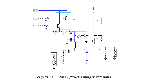
The power
amplifier consists of the Siemens SIEGET® BFP450 wideband
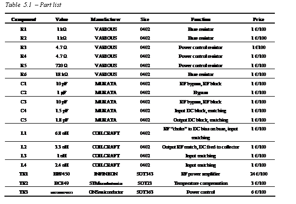
transistor, operating in class-AB (see Figure 5.1 and Table 5.1). The BFP450
has two emitter-leads which have to be carefully grounded to ensure stable
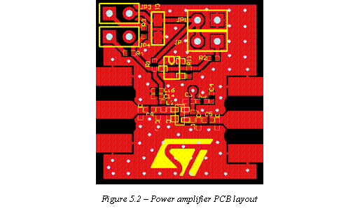
operation and performance according to the specifications. The PCB layout (see
Figure 5.2) of the amplifier results in an emitter-to-ground inductance of 130
pH (typical value).
5.2 DESIGN MODEL
The solver software used is
Ansoft DesignerTM SV ver. 1.0.
The model is shown in Figure
5.3, as we discussed to in chapters 2 and 3 the transistor is completely
characterized with S parameters and thanks these parameters is possible to find
optimum source and load impedances either for simultaneous conjugate matching.
Thanks to
BFP450 simulation model given by INFINEON and with the help of Smith Tool of
Ansoft Designer SV has been possible to find optimal and very light
input/output matching networks, as shown in Figure 5.1 and Table 5.1.
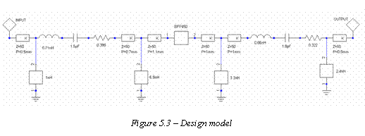
Figure 5.4
shows the source (GMS) and load (GML) reflection coefficients found by
simulation. Now, all that remains is to surround the transistor with components
that provide it with source and load impedances “look like” GMS and GML.
For the input/output matching
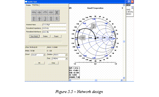
network design we used Smith Tool of Ansoft Designer SV. Figure 5.5 shows the
input matching network design. The object of the design is to force the 50-ohm
source to present a reflection coefficient of
![]() . With GMS
. With GMS

plotted as
shown, the corresponding desidered and normalized impedance is read directly
from the chart as ZS = 0.06 –
j0.18 ohm. Remember, this is a normalized impedance because the chart has
been normalized to 50 ohms. The actual represented by GMS is equal to 50(0.06 – j0.18) = 3 – j9 ohms. To force
the 50-ohm source to actually appear as a 3
– j9 ohms impedance to the transistor, we only
add a shunt and a series reactive component as shown on the chart of Figure
5.5.
Of course,
that is very simple design, indeed, it does not consider the real models of
components and the PCB. COILCRAFT® and MURATA® provide,
respectively, S parameters of inductors and equivalent circuit (LCR) of
capacitors. With these simulation models and with Trasmission Line Model of
Ansoft Designer SV is possible to design matching networks with results close
to the reality.
Well, the second step is to
find the matching networks with real models. That was done with the help of
Smith Tool of Ansoft Designer SV and testing more values of components in
simulation. The result is shown in Figure 5.6.
5.3 THE POWER AMPLIFIER ANALYSIS

Thanks to the use of Ansoft
Designer tools we found good matching networks, the S11 and S22,
at 2.45 GHz, are shown in Figure 5.6.
The next step is to analyse
the model shown in Figure 5.3 to have some report about gain, stability factor,
S11, S22, forward gain and input output return loss.
Figure 5.7 shows the gain
from 0.5 to 3 GHz. At 2.45 GHz we have a gain equal to 11.93 dB. The fact that
the gain of PA at low frequency is higher than high frequency does not amaze
because the gain of BFP450 decreases when the frequency increases. At 2.45 GHz
we have the highest gain possible at that frequency.
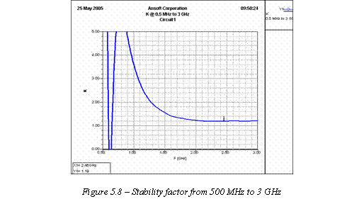
The stability factor at
varius frequency is shown in Figure 5.8. In bluetooth band, K is greater than 1, then the PA is unconditionally
stable. From 600 to 650 MHz, K is
less than 1, therefore the PA is potentially unstable and will most likely
oscillate. At 2.45 GHz K is equal to 1.19.
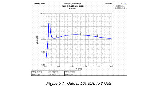
Figure 5.9
shows the forward gain in the range of 0.5 to 3 GHz. As well as expected at
2.45 GHz we have the maximum (-17.29 dBm).
Figure 5.10 shows the
input/output return loss. Also in this case, we have the best value at 2.45
GHz, indeed the input/output ports are tuned to 50 ohms.
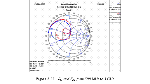
Finally, Figure 5.11 shows
S11 and S22 at various frequencies. Obviously, they are close to 1 at 2.45 GHz.
When we move from that frequency, we lose the optimum matching (50 ohms).
5.4 THE BFP450 POWER AMPLIFIER MEASUREMENTS
Measurements were performed
using a signal generetor, a spectrum analyzer and a network analyzer. The power
meter was used to calibrate the cables. A photo of the test setup is shown on
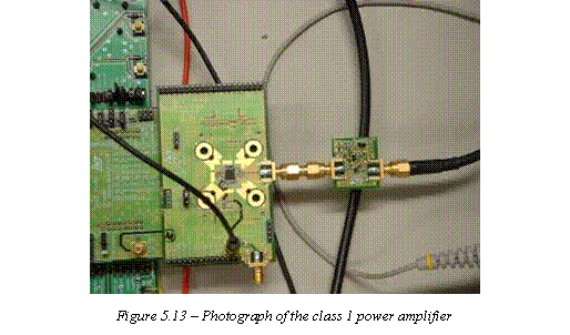
Figure 5.12, while Figure 5.13 shows a photo of class 1 power amplifier.
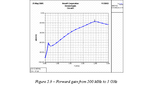
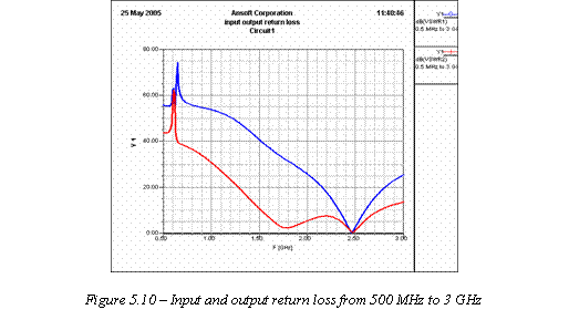
Figure 5.1 shows the
schematic with optimum matching networks. The schematic is
complete of
power control and PA enable. As the START499 PA, the measurements was done
under a determinate range of temperature, power supply and input power. Despite
the design was done for a biasing current equal to 12 mA, also other current
values was investigated. Of course, the best results were found with Icq = 12 mA.

Figure 5.14
shows the output power as function of input power at varius Icq. We can notice that with a biasing
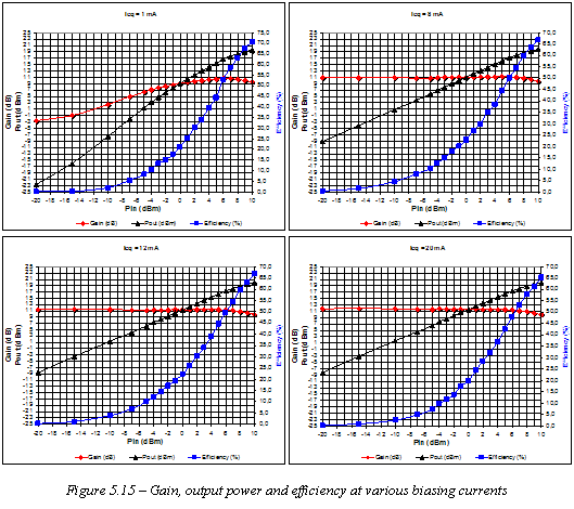
current equal to 8, 12 and 20mA we have similar results, nevertheless, as shown
in Figure 5.15, with different efficiency values.
Also in this
case, the efficiency is high with low biasing currents. But, the efficiency
with Icq = 12 mA is around 70 %,
higher than with START499.
At every biasing current, the
maximum 1 dB compression point value is around 21 dBm.
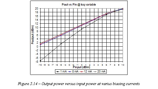
Figure 5.16
shows gain, output power, and efficiency versus input power at
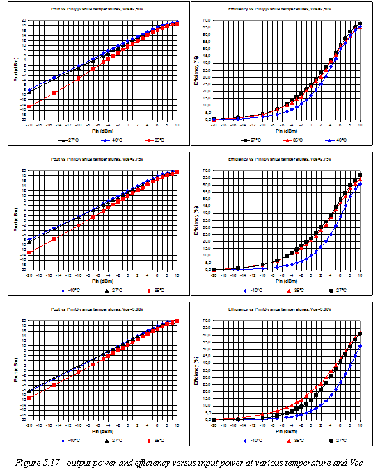
Figure 5.17 shows output
power and efficiency versus input power at various temperature and Vcc. As we
can notice, with low temperature, the gain is higher than high temperature,
like the START499, but, the efficiency is worse.
There are
not essential differences at varius Vcc, but, the RF performance depends,
heavily, on temperature.
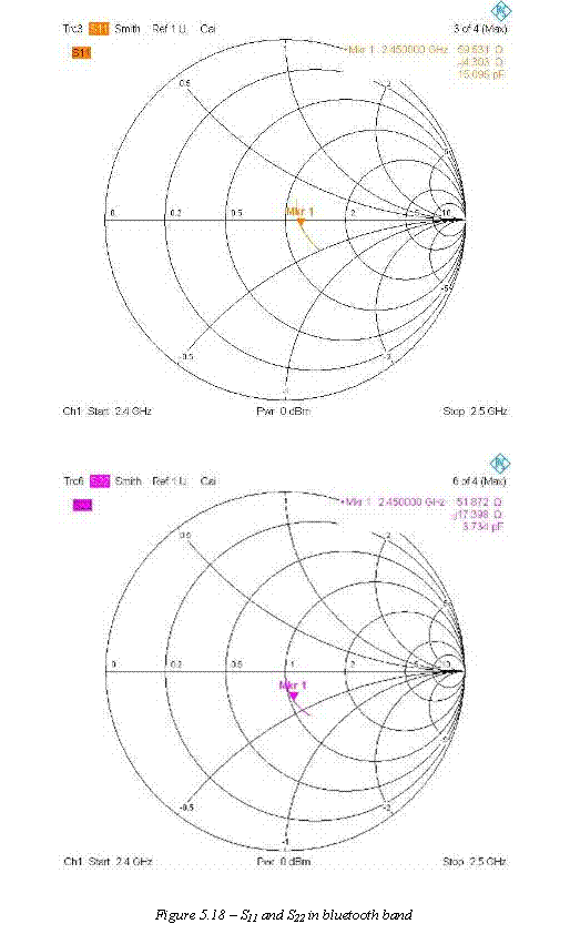
At last, Figure 5.18 shows S11 and S22 in bluetooth band, notice the marker at 2.45 GHz.
Comparing these results with those got from linear analysis, we can see
analogy.
5.5 THE BFP450 POWER AMPLIFIERS DISCUSSION
Amplifier tune-up is
accomplished by adjusting matching networks for maximum output power with
minimum collector current. The amplifier tunes in bluetooth band 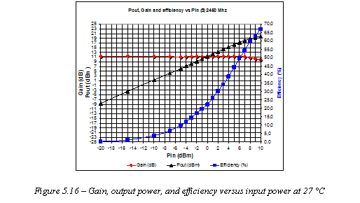
while
mantaining as S11 and S22 a value close to 1
(Figure 5.18). Note from Figure 5.7 that the bandwidth is further 100 MHz with
the amplifier tuned to a center frequency of 2.45 GHz.
We designed the Class1 power
amplifier to be most efficient possible PA in the bluetooth broadcast
marketplace with a cost lowest.
The exceptional efficiency
(70 %) of PA gives a competitive advantage. It can be used in battery powered
applications where the power consumption is a key factor.
The measurements were focused
on characterization of the bias and temperature dependance. A comparison of
gain, output power and efficiency measured at room temperature and at high
temperature shows large differences as reported in Figure
5.17. At temperature below zero, with any voltage supply, the efficiency
degraded. These measurements suggest the importance of temperature and voltage
supply effect on the class-AB amplifier characterization. As well as the
START499, changing the base resistor of bias transistor (BC849) a better
temperature stabilization is possible, but this causes efficiency degradation.
To have the best RF
performance from BFP450, it must work at high output power.
Finally, with BFP450 power
amplifier the challenge was won, we have a small size amplifier with a light
BOM, with low power consumption and with
very low cost.
