A few years ago I built this simple interface to acquire
analog signals into the TRS.
The main purpose was to read values of temperature for a
study about weather conditions, but I have to admit I later used
the same unit for projects such as reading analog joysticks.
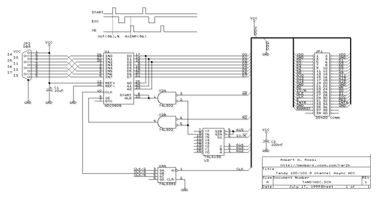
Circuit Description
The ADC plugs into the Bus Expansion connector in the back
of the 102. Since the pinout of the B.E. on the 100 is identical
as far as the logic signals used by this interface, I used it
on both models without any problem.
It must be considered that this unit is intended ONLY for
applications where signals change relatively slowly, and a resolution
of 8 bit is sufficient.
From a software viewpoint, the ADC is initialized by performing
an OUT (96), N [N=input channel to be read 0%7; only the 3 lsb
are used]. This generates a Start pulse for the ADC0808 which
selects the input and starts the conversion. Because of the relarively
slow speed of BASIC, by the time the instruction is completed
and the TRS is executing the next one, the ADC has completed
the conversion. To read its content, it is sufficient to perform
an input with VAR=INP(96).
Because the EOC (End of conversion) signal generated from
the chip when a conversion has ended is ignored, we cannot be
100% sure that the number we're reading is indeed the very last
value from the channel we've just selected; in order to achieve
such goal, we should wire EOC back into the TRS through a second
input port. This solution was not implemented because it requires
more hardware, and it uses one more I/O address, causing potential
conflicts with other custom designed interfaces. To ensure a
correct reading, it is sometimes advisable to insert a delay
between Out and In, particularly after switching from one channel
to another.
The ADC is driven at 600KHZ:1/4 the speed of the 80C85.
Analog signals can be applied to JP2.
Notes
The address "96" was chosen arbitrarely among the
ones not used from the TRS. U3 performs the addressing; it is
possible to alter the diagram to use a different I/O.
To drive the ADC8080 at full speed (about 1Mhz, depending
on the manufacturer), an internal oscillator could be used instead
of the clock divider.
The input range is set to 0%5V by the levels applied to Vref-
and Vref+. Refer to the ADC0808 datasheet to learn how to adjust
it to your needs.
The inputs of the ADC08XX family are extremely sensitive
to negative voltages. If there's any possibiliy of such, make
sure to provide some protection (i.e. dual diode)
A challenge for the bold
If the unit were to be built INSIDE the TRS80 (there's room,
don't worry), the EOC signal from the chip could be connected
to one of the unused input bits of the same port that handles
the bar code reader providing a way of a faster and more accurate
acquisition even in assembler.
In spite of the recommendations for the ADC0808, I have run
it at 1/2 the clock speed (1.2MHZ) without noticing any problem.